T1: Why Standards Matter: Impact and Importance of IEEE Standards
Abstract: Almost every human on the planet today interacts with technology as part of their day and these technologies are built around a strong foundation of Standards. The IEEE Standards Association is at the forefront of developing standards across various technology sectors with very high impact standards such as WiFi (802.11), Ethernet (IEEE 802.3), Power and Energy Standards such as IEEE 1547 on Distributed Energy Resource and several others in the areas of Generation, Transmission and Distribution, Healthcare (IEEE 11073), Vehicular Technology Standards, Aerospace, Biomedical, EMI/EMC to name a few. More recent advances in technologies such as AI/ML and the digital transformation that is taking place in society and all around us has given rise to new sets of challenges that IEEE SA has been addressing to build trust in systems by focusing on cyber security, identity, and privacy and with a strong focus on socio-technical standards around Ethics of AI, Children online frameworks and Sustainability. The talk will provide insights into the importance of standards development and its impact on technology advancement, and adoption in both current and emerging technologies. Also touched upon will be certification of products and standards education which provides key aides to students and faculty. The session will discuss a practical approach to how you can be part of the IEEE standards development. Sri Chandra (Country Head, IEEE India office and Lead - Foundational Technologies Practice, IEEE SA) will present the session covering all aspects of standards development to show how one can get started and get involved.
Speaker:
Srikanth Chandrasekaran
Country Head – IEEE India
Global Practice Lead, Foundational Technologies, IEEE Standards Association
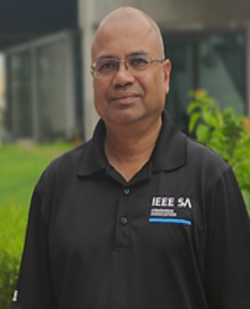
About Speaker: Sri has been associated with the IEEE for the past 10 years focused on developing key standardisation programs that address core issues of security, identity, trust and building end-to-end trustworthy devices and systems across emerging areas such as IoT/Smart Cities, Quantum Computing, Artificial Intelligence & Machine Learning, Sensors and Blockchain. Sri also heads the standardization efforts for IEEE SA for the Asia Pacific region and has recently taken additional charge of leading the IEEE India Business Operations. As part of the programs in India, Sri leads the IEEE Blended Learning Program initiative, an eLearning platform, focused on bridging skills for students in emerging technologies and lateral skilling of industry professionals. Prior to joining IEEE, Sri was associated with Freescale Semiconductor Inc. (formerly Motorola Inc.) for 17 years, managing a global Electronic Design Automation R&D team based out of Adelaide Australia. Sri received the Accellera Technical Excellence Award in 2009 for his leadership and contributions to design automation standardisation. Sri holds a Bachelor of Science degree in Physics from Madras University, India and Master’s degree in Electrical Communication from Indian Institute of Science, Bangalore, India.
T2: Machine Learning in EDA Tool Development: An FPGA Based Study
Abstract: As the technology node size decreases, due to Moore’s Law and Dennard’s scaling, more and more transistors are fitted per unit area inside the integrated circuit (IC) than ever before. With the decrease in technology size, the tools used to design ICs are becoming more complex. While designing an IC, it is always a good practice to estimate the power, performance, area (PPA), congestion, and wirelength of the design down the flow in an early stage. Traditionally, this is done using statistical, mathematical, or analytical methods. The analytical and mathematical models are computationally complex and have lower accuracy. These methods generally solve every problem from scratch and do not utilize any experience or knowledge. Machine learning is emerging fast, and in the last five to six years, the application of ML has penetrated the EDA domain. All the problems previously solved using analytical methods are now reframed as ML problems. The same issues, which took a few minutes to hours using analytical or mathematical methods, can now be solved using ML-based pre-trained models within a few seconds. Machine learning has found its application in almost all stages of IC designs, including timing, power, and area estimation; routing congestion estimation using classical ML and deep learning methods; design space exploration; CAD tool parameter tuning; WL estimation and lithographic hotspot detection. This tutorial aims to explore the application of machine learning techniques to address various challenges within Electronic Design Automation (EDA). The tutorial focuses on leveraging machine learning to tackle specific issues across five key areas within EDA:
- 1. Power, Performance, and Area Prediction in RTL and HLS Designs
- 2. Design Space Exploration (DSE)
- 3. CAD Tool Optimization Using ML
- 4. Congestion Estimation in HLS and RTL Designs
- 5. Use of Machine Learning in FPGA Physical Design Flows
Speaker:
Dinesh Bhatia
University of Texas at Dallas, USA

About Speaker: Dinesh Bhatia is a faculty member in the Erik Jonsson School of Engineering and Computer Science at the University of Texas at Dallas. He directs research activities within the IDEA Lab. Currently, he serves as Department Head of the Department of Electrical and Computer Engineering. His research investigations have spanned the areas of high-performance computing, healthcare & medical devices, and power and energy systems. He has published extensively in Architecture and Computer-Aided Design for Field Programmable Gate Arrays (FPGAs). He has served on technical program committees of several international conferences related to FPGAs, field-programmable technology, and system-level design using FPGAs. He has experience in building large-scale custom computing and embedded systems. These include the principal designer and investigator for the RACE system for Wright Laboratories of USAF, the principal investigator for DARPA funded REACT program, and several more. In the area of power and energy systems, he has primarily worked in the areas related to power converters. Recent research has resulted in breakthrough results and the founding of a startup company, Cirasys Corporation. Cirasys has received initial funding from NSF, UT System, and Texas Emerging Technology Fund. He is an architect of several patient monitoring solutions in medical devices and healthcare. He has served on the editorial board of IEEE Transactions on Computers, as general chair for International Conference on Body Sensor Networks, and was IEEE Circuits and Systems society’s distinguished lecturer for 2007-2008. He has served on Technical Program committees of several conferences. He is a senior member of IEEE, IEEE Engineering in Medicine and Biology Society, IEEE Circuits and Systems Society, ASEE, AAAS, Eta Kappa Nu, and the honor society of Phi Kappa Phi. He is experienced in IP litigation and has participated in technology evaluation for startups and small businesses. His research focus includes Architecture and Computer-Aided Design for Field Programmable Gate Arrays (FPGAs), Electronic Design Automation, Reconfigurable Computing, Custom Computing Systems with applications in resilient and trustworthy deep learning, and domain-specific architectures, Medical Electronics, Personal Medical Devices, AI in Medicine. Education: Ph.D. – Computer Science, The University of Texas at Dallas, 1990 M.S. – Computer Science, The University of Texas at Dallas, 1987 B.E. – Electrical Engineering, National Institute of Technology, Suratkal, India, 1985 Affiliations: IEEE, Senior Member, IEEE Engineering in Medicine and Biology Society, IEEE Circuits and Systems Society, ASEE, AAAS, Eta Kappa Nu, The Honor Society of Phi Kappa Phi
T3: Design-For-Manufacturability for Nano-Scale CMOS Technology
Abstract: In semiconductor manufacturing, physical design is a process of turning a circuit into geometric shapes (layout), which will be manufactured onto the wafer in various chemical, mechanical and electrical steps. As geometric feature sizes continue to shrink, it is difficult to fabricate these shapes precisely onto the wafer without any defects. Manufacturing constraints must be applied during the physical design phase. It has become increasingly important to have access to different types of physical verification and enhancement tools that can check a design's manufacturability, identify any possible defects, and fix them. These products are known as Design for Manufacturability (DFM) tools. The seminar presents the different types of DFM tools and how deep learning techniques can help to accelerate the development of DFM tools.
Speaker:
Yongfu Li
Institute of Microelectronics of The Chinese Academy of Sciences, China
 About Speaker: Yongfu Li (S’09–M’14-SM’18) received the Ph.D. degrees from the Department of Electrical and Computing Engineering, National University of Singapore (NUS), Singapore. He is currently a Professor in Institute of Microelectronics of The Chinese Academy of Sciences, China, China. He was a research engineer with NUS, from 2013 to 2014. He was a senior engineer (2014-2016), principal engineer (2016-2018) and member of technical staff (2018-2019) with GLOBALFOUNDRIES, as a Design-to-Manufacturing (DFM) Computer-Aided Design (CAD) research and development engineer. He has involved in different roles in many prestigious IEEE CASS conferences (ISCAS, ISICAS, AICAS, NEWCAS, ISVLSI, ASP-DAC, and APCCAS) and regional activities. He has organized several special sessions and issues in IEEE CASS Journals and Conferences. Currently, he is serving as the IEEE CASS Board of Governors (R10 Member at Large), IEEE CASS Standard Activities Sub-Division Chair-Elect, and IEEE Open Journal of Circuits and Systems Associate-Editor-In-Chief.
T4: Selecting the Right Topology of Voltage Regulators for Your System
Abstract: A voltage regulator or dc-dc converter is an essential block of an electronic system. With the growing demand of high-performance voltage regulators in the consumer market, one-third of $30bn power market is contributed by the voltage regulators and is expected to get double in the next 5 years with the rising demand for automotive, solar, LED lighting, and mobile applications. The design specifications of these regulators usually depend upon the application. For instance, the input/output and current requirement of voltage regulators used in automotive applications could be completely different from the one used in a mobile phone. Furthermore, the type and number of regulators used within the same system may also vary based on the requirements of various modules or sub-systems. While a mobile phone requires supply voltage ranging from 0.8V to 30V generated from a single Li-ion battery, a LED bulb may require to generate 60-70V from 220V rms, and power supplies for automotive and server applications are usually generated from a 12V input source. The load current needed by a processor and audio/power amplifiers may be the order of a few amperes while the current needed by sensors and other analog circuits could be limited to a few 10s of mA. Therefore, under such a wide variation of input/output voltage and load currents, it becomes quite challenging to choose between switching (dc-dc converter) and linear regulator. The availability of the number of topologies within the same type of regulator makes it even more difficult which sometimes may lead us to select the wrong topology which fails to meet our performance or cost requirement. In this tutorial, we will discuss various types of regulators such as linear vs switching, inductive vs capacitive, isolated vs non-isolated, discrete vs in-chip etc., and choose the best voltage regulator for different applications. Based on the performance requirement such as efficiency, noise, and load/line transient, the proper selection of the regulator’s control and power stage topology is also discussed.
Speaker: Dr. Qadeer Ahmad Khan Integrated Circuits and Systems Group, Department of Electrical Engineering, Indian Institute of Technology Madras, India.
About Speaker: Dr. Qadeer Khan is an assistant professor in the Integrated Circuits and System group of the department of Electrical Engineering, Indian Institute of Technology Madras. He received his Bachelor's degree in electronics and communication engineering from Jamia Millia Islamia University, New Delhi, India, in 1999 and the Ph.D. degree in electrical and computer engineering from Oregon State University, USA in 2012. His Ph.D. work was focused on developing novel control techniques for high performance switching dc-dc converters. From 2012 to 2015, he worked as a Staff Engineer, Power Management Systems with Qualcomm, San Diego and from 2015 to 2016 with Qualcomm, Bangalore
T5: Multi-channel Delta-Sigma Analog-to-Digital Converters Without Reset
Abstract: Modern sensor systems in biomedical, instrumentation, and industrial control systems require information from multiple sensors to be digitized and processed. This demands a multi-channel analog-to-digital converter (ADC). This is often implemented by multiplexing the inputs, digitizing the multiplexed stream using a single ADC, and demultiplexing the digital bits. To realize high resolutions, the common choice is to use a noise-shaping ADC, like delta-sigma ADC (DS-ADC). But, due to the long impulse response of the decimation filter needed in these noise-shaping ADCs, they have a long memory of the past inputs. Hence, when used directly in multiplexed environments, there will be severe cross-talk ( -13dBc) between the output channels. One way around this problem is to use an incremental DS-ADC, where the ADC is reset periodically to clear its past memory. This intermittent operation compromises the signal-to-quantization noise ratio (SQNR) and the signal-to-thermal noise ratio (SNR). As an alternative, schemes have been proposed that do suitable modifications only to the digital filter and (or) add a front-end sample-and-hold so that the DS-ADC can be run continuously without reset. These techniques adopt general principles of multi-rate signal processing to realize the desired time-invariant transfer functions between input and output. Besides their application to reset-free multi-channel ADCs, understanding multi-rate signal processing is of intrinsic value to circuits and systems engineers.
In this tutorial, the techniques to realize reset-free multi-channel delta-sigma ADCs will be discussed. Based on this, the pros and cons of both the reset-free and incremental DS-ADCs will be elucidated. In addition, some recent developments in incremental delta-sigma ADCs will also be briefly discussed. This will be of practical importance to circuit designers to make calculated decisions on choosing the right architecture for a given application. This is also relevant given that the need for such multi-channel sensor acquisition systems is growing rapidly and is only going to increase further.
Speakers:
R. S. Ashwin Kumar, Indian Institute of Technology Kanpur, India
Nagendra Krishnapura, Indian Institute of Technology Madras, India
About Speakers: R. S. Ashwin Kumar received the B.E. degree from the College of Engineering, Guindy (CEG), Anna University, Chennai, India, in 2013, and the Ph.D. degree from IIT Madras, Chennai, India, in 2020. He is currently an Assistant Professor with IIT Kanpur, Kanpur, India. His research interests are in analog & mixed-signal IC design and signal processing.
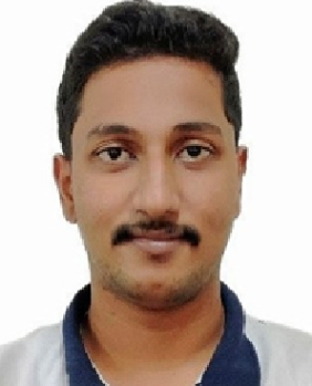 Nagendra Krishnapura obtained his BTech from the Indian Institute of Technology, Madras, India, and his PhD from Columbia University, New York. He has worked as an analog design engineer at Celight, Multilink, and Vitesse semiconductor. He has taught analog circuit design courses at Columbia University as an adjunct faculty. He is currently a professor at the Indian Institute of Technology, Madras. His interests are analog and RF circuit design and analog signal processing.
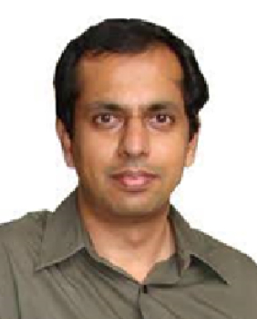
T6: A Reliable and Robust Framework for Accurate Timing Sign-Off With Reduced Design Margin of Digital Integrated Circuits
Abstract: In this tutorial, we discuss circuit performance estimation approaches considering PVT/temporal and layout dependent effects (LDEs) at a very early (pre-layout) stage. These approaches involve development of circuit performance models usable by designers. The emphasis is on timing performance of digital circuits for the performance prediction and development of robust and scalable digital and mixed signal designs while targeting desired performance parameters. We endeavour to develop a general framework which quantitatively and directly links the device/layout level parameters to circuit performance, and on the other hand, is physics and/or circuit topology based. We address this by identifying the critical terminal voltages for a circuit at which its charging/discharging mechanism changes. This general framework is based on the change of the region of operation of one or more transistors in a circuit topology during transitions. Therefore, this approach is portable across process design kits (PDKs) of several foundries and across CMOS technology generations. The circuit performance models of combinational and sequential cells have been applied in diverse areas such as a reduction of standard cell re-characterization due to PVT/aging variations and LDE, static timing analysis (STA) of digital circuits with an in-situ consideration of device-level variations such as aging. Then these performance prediction models are used for robust and scalable digital and mixed signal design such as ring oscillators (ROs), voltage-controlled oscillators (VCOs), clock buffers, and time to digital converters (TDCs). A robust framework considering reliability for accurate timing sign-off with reduced design margin of digital integrated circuits.
Speakers
Dr. Anand Bulusu
Professor, Department of Electronics and Communication Engineering, Indian Institute of
Technology Roorkee, India
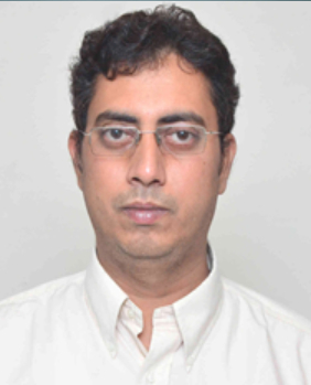 About Speaker: Anand Bulusu (Member, IEEE) received the Ph.D. degree from the Indian Institute of Technology Bombay, Mumbai, India, in 2006. From 2007 to 2008, he worked as a Senior Research Engineer with the Silicon Technology Solutions Groups of Freescale Semiconductor (currently NXP Semiconductor). He is currently working as a Professor with the Department of Electronics and Communication Engineering, Indian Institute of Technology Roorkee, Roorkee, India. His current research interests include device physics, circuit performance models and design, device-circuit interaction for emerging and conventional devices, and digital/analog/mixed-signal circuit design.
Industry Tutorial 1: Building Energy Efficient Wireless Semiconductors and Systems
Abstract: A common requirement in electronic devices is an extended battery life. Complex SoCs, the core of most electronic systems, have seen a tremendous amount of advancement in the methods used to reduce power consumption. This tutorial gives an in-depth look at these, which include techniques to isolate and regulate power in internal processing elements at low granularity and enabling a combination of software and hardware to achieve unprecedented efficiencies. It also covers the smart use of protocol supported sleep states for achieving long battery life while keeping the end-application requirements well met, showing how battery life enhancement is a joint endeavour involving semiconductor device construction and control, the simultaneous use of multiple architecture level techniques, and effective use of standards defined features.
Speaker:
Joseph Kolapudi
Silicon Labs, Hyderabad
 About Speaker: Joseph Kolapudi is Associate Engineering Manager at Silicon Labs, Hyderabad, coming in through its acquisition of Redpine Signals. Joseph has over eight years of experience in Applications Engineering, enabling customers to build IoT solutions using the company's Wi-Fi and BT chipsets and modules. He areas of expertise include developing IoT applications to showcase the connectivity and energy efficiency of the chipsets, interfacing the Wi-Fi chips to a multitude of external MCUs, and Wi-Fi 6 for IoT. He has helped create the company's offering for Matter over Wi-Fi, Matter being the new IoT standard developed by the Connectivity Standards Alliance. Joseph has also been responsible for developing and delivering training for the company's world-wide Field Application Engineers.
Industry Tutorial 2: Design, Test and Calibration of High-accuracy CMOS Temperature Sensors
Abstract: Speaker: Sudhakar Singamala Rajashekar Benjaram About Speaker: